SPM Research
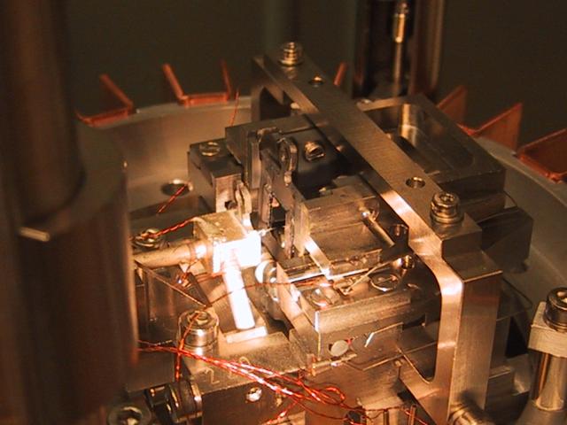
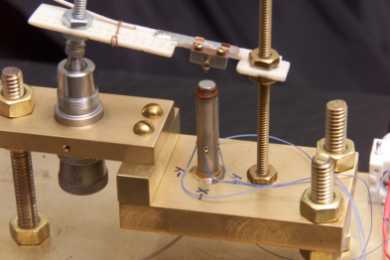
The microscope consists of a "head," which is the electro-mechanical system for carefully controlling the relative separation and position of the tip and sample, and the controller, which processes the electrical signals using hardware and software to create the image of the surface. A simple STM head can be made fairly easily (see image of a brass STM head at upper right), and more sensitive heads can be made or purchased, such as the Omicron STM1 head shown at left.
The AFM operates by measuring the electrostatic forces between the tip and the surface and can image the surfaces of metals, semiconductors, and insulators. While obtaining atomic-resolution images with AFM can be challenging, its use for imaging all material types at the nano to micro-meter scales has made AFM very popular for characterizing material surfaces.
The term SPM can be used to encompass all of the many imaging techniques that have extended or enhanced basic STM and AFM. These SPM techniques have been enable a range of surface material properties to be mapped or "imaged" qualitatively and sometimes quantitatively. In our research, we commonly use the SPM techniques to learn more about the structure, composition, and properties of new materials that we make in the lab.
Below are SPM images from our research. Click the images to see a
larger version.
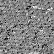
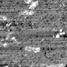
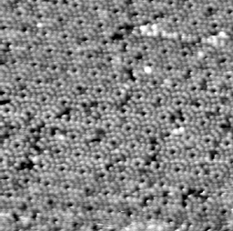
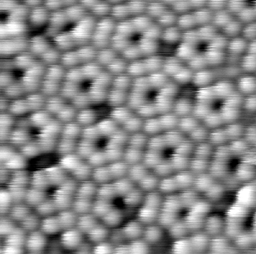
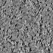
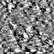
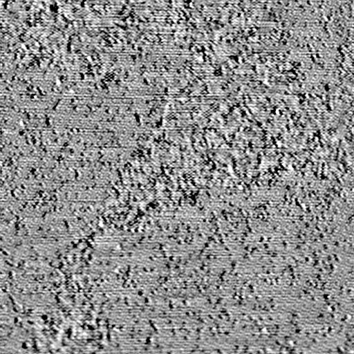
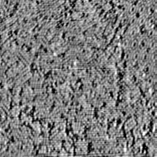
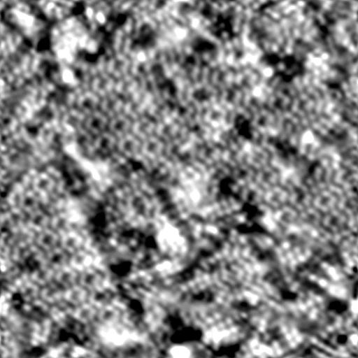
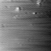
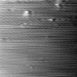
SPM Images
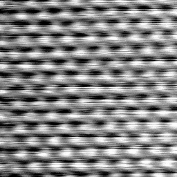
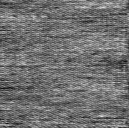
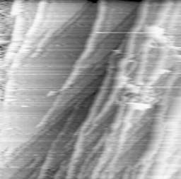
- Omicron VT-STM Image of Br-Si(100)-(2x1) in UHV at 720K:
50.0 x 50.0nm2
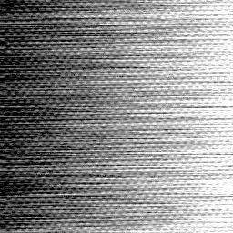
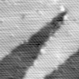
- Dual-bias Omicron VT-STM Images of Si(111)-(7x7):
57.0 x 57.0nm2
+2V,200pA57.0 x 57.0nm2
-2V,200pA
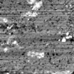
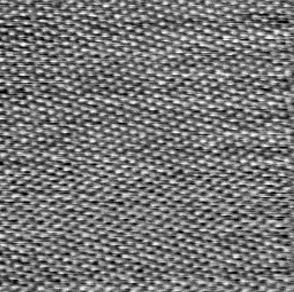
- Omicron STM 1 Images of Si(100)-(2x1) in UHV:
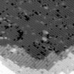
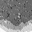
50.0 x 50.0nm2 30.0 x 30.0nm2 25.0 x 25.0nm2 Derivative + Topography
25.0 x 25.0nm2Clean surface
50.0 x 50.0nm2
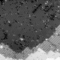
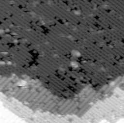

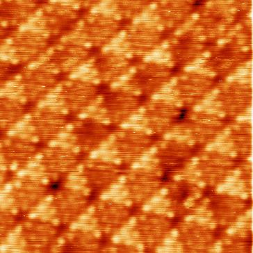
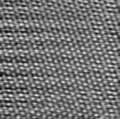
- Omicron STM 1 Images of Si(111)-(7x7) in UHV:

50.0 x 50.0nm2 30.0 x 30.0nm2 10.0 x 10.0nm2
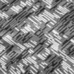
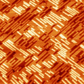
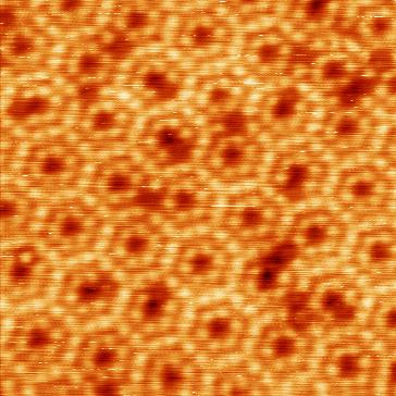
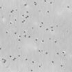
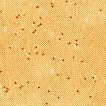
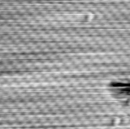
- Omicron STM 1 Images of HOPG in UHV:
1.5 x 1.5nm2 5.0 x 5.0nm2 7.5 x 7.5nm2 15.0 x 15.0nm2

- AutoProbe VP Images of Si(111) and Ge(111) in UHV:
100.0 x 100.0nm2 50.0 x 50.0nm2 30.0 x 30.0nm2
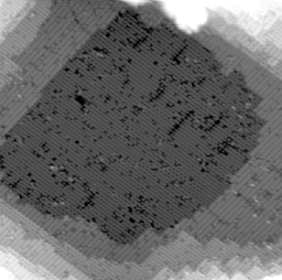
- AutoProbe VP Images of GaAs(110) in UHV:

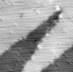

20.0 x 20.0nm2 350.0 x 350.0nm2 25.0 x 25.0nm2 12.0 x 12.0nm2
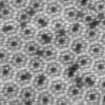
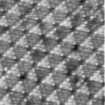
- AutoProbe VP Images of HOPG in Air:
2.0 x 2.0nm2 8.0 x 8.0nm2